Position Description
Optical Memristors are disruptive photonic elements which have attracted significant attention during the last few years, while offering unique switching and memory-like characteristics, for driving the future optical networks and sensing systems. The FORTH-SYNERGY project Optical Memristors, based on Photo-fluidity, Chalcogenide Whispering Gallery Mode Cavities (OMEGA) proposes the elaboration of an optical memristive component, fusing together the exotic photo-sensitivity properties of chalcogenide glasses (ChGs) and the extreme power accumulation and modal state density of whispering gallery modes (WGMs) resonation inside spheroid microcavities.
A highly competitive, post-doctoral research fellow is sought for the project OMEGA, for 12 months initial contract, with an additional up to 12 months, extension foreseen upon performance. The successful candidate must have a PhD degree in Physics or Electrical/Electronic Engineering, with a strong experimental/theoretical background in Optical Fiber Devices and/or Whispering Gallery Mode systems, being proven by publications record, previous experience and/or thesis subject and reference letters. The applicants must provide at least two names (preferably three) of academics who can provide reference letters. Previous background on Glass science/photosensitivity will be considered as a strong asset. Applications without satisfying the above criteria will not being considered.
For the full announcement, follow the link "Related Documents"
Required Qualifications
- PhD degree in Physics or Engineering
- Experience in optical fiber devices
- Experience in whispering gallery mode systems/physics
- Materials/glass science/photosensitivity
- Working knowledge of English
Application Procedure
Applications received before July 3rd 2020 will receive immediate attention; however, applications will be reviewed thereafter until the position is filled.
Interested candidates who meet the aforementioned requirements are kindly asked to submit their applications to the address (hr@iesl.forth.gr), with cc to the Scientific Coordinator Dr Stavros Pissadakis (pissas@iesl.forth.gr).
In order to be considered, the application must include:
- Application Form (Form Greek or Form English to the left)
- Detailed CV and list of publications
- Names of three academic referees
- Scanned copies of academic titles
Applications will be reviewed till the position is filled
Appointment Duration
12 monthsAbstract
SnS crystals (Tin Sulfide), item:1
Tin Selenide (SnSe), item:1
Germanium Sulphide (GeS), item:1
Tungsten Disulfide (WS2), item:1
Tungsten Diselenide (WSe2), item:1
h-BN (Large size), item:1
Technical Characteristics
SnS crystals (Tin Sulfide), item:1
Characteristics of vdW SnS crystals
Crystal size: 10mm or larger
Materials properties: Indirect gap semiconductor
Crystal structure: Hexagonal
Unit cell parameters: a = b = 0.368, c= 0.582 nm, α = β = 900, γ = 1200
Growth method: [Default] Flux zone (no halide contamination) defect free
[Optional chemical vapor transport] Halide contamination is common
Purity: 99.9999% confirmed
Tin Selenide (SnSe), item:1
SnSe single crystals characteristics
Crystal size: 1cm in size
Materials properties: Thermoelectric semiconductor (anisotropic semiconductor)
Crystal structure: Pnma [62]
Unit cell parameters: a = 0.421nm, b = 0.452 nm, c= 1.181 nm, α = β = γ = 900
Growth method: Bridgman growth technique
Purity: 99.9999% confirmed
Germanium Sulphide (GeS), item:1
Crystal size: Larger than 1cm
Materials properties: 1.65 eV semiconductor, anisotropic 2D material
Crystal structure: Orthorhombic
Unit cell parameters: a = 1.453, b = 0.365nm, c= 0.435 nm, α = β = γ =900
Growth method: Flux zone (guaranteed no halide contamination)
[On request: chemical vapor transport (CVT) contains Br2, Cl2, TeCl4, and other halides]
Purity: 99.9999% confirmed
For the cases of Tin Sulfide (SnS), Tin Selenide (SnSe) and Germanium Sulphide (GeS), high quality bulk crystals are required for series of experiments. There are reports with different experimental results for these crystals indicating that products differ with respect to the company that develops them. We have preliminary results using crystals from “2D semiconductors” and for consistency we would like to purchase from the same company.
Tungsten Disulfide (WS2), item:1
Typical characteristics of WS2 crystals from 2Dsemiconductors
Crystal size: ~1cm in size
Dopants: Undoped (intrinsic semiconductor)
Materials properties: 2.02 eV emission (300K), direct gap semiconductor
Crystal structure: Hexagonal phase
Unit cell parameters: a = b = 0.317nm, c= 1.230 nm, α = β = 900 , γ = 1200
Growth method: [Default] Flux zone (no halide contamination) defect free
[Optional CVT]: Contains Br2, Cl2, TeCl4, and other halidesPurity: 99.9999% confirmed
Purity: 99.9999% confirmed
Tungsten Diselenide (WSe2), item:1
Characteristics of WSe2 crystals from 2Dsemiconductors USA
Crystal size: ~1cm in size
Dopants: Undoped (intrinsic semiconductor)
Materials properties: 1.62 eV emission (300K), direct gap semiconductor
Crystal structure: Hexagonal phase
Unit cell parameters: a = b = 0.331nm, c= 1.298 nm, α = β = 900 , γ = 1200
Growth method: [Default] Flux zone (no halide contamination) defect free
[Optional CVT]: Contains Br2, Cl2, TeCl4, and other halides
Purity: 99.9999% confirmed
h-BN (Large size), item:1
The properties of large size h-BN crystals
Sample size: Contains 3-4 crystals. Each measure < 5mm in size
Materials properties: 2D dielectric / insulator
Production method: Epitaxial solidification technique
Characterization method: SIMS, XRD, EDS, Raman (see product images)
For the cases of WS2, WSe2 and h-BN crystals, adding to consistency which is important to our experiments as we stated before, we would like to acquire crystals grown with flux zone method. We want to study the communication between flake of different crystals and it is reported that this phenomenon is more likely to happen for crystals grown with the referred method. “2D Semiconductors” offer high quality flux zone crystals that we think will be the optimal choice for our experiments.
Procedure
SnS crystals (Tin Sulfide), item:1
Characteristics of vdW SnS crystals
Crystal size: 10mm or larger
Materials properties: Indirect gap semiconductor
Crystal structure: Hexagonal
Unit cell parameters: a = b = 0.368, c= 0.582 nm, α = β = 900, γ = 1200
Growth method: [Default] Flux zone (no halide contamination) defect free
[Optional chemical vapor transport] Halide contamination is common
Purity: 99.9999% confirmed
Tin Selenide (SnSe), item:1
SnSe single crystals characteristics
Crystal size: 1cm in size
Materials properties: Thermoelectric semiconductor (anisotropic semiconductor)
Crystal structure: Pnma [62]
Unit cell parameters: a = 0.421nm, b = 0.452 nm, c= 1.181 nm, α = β = γ = 900
Growth method: Bridgman growth technique
Purity: 99.9999% confirmed
Germanium Sulphide (GeS), item:1
Crystal size: Larger than 1cm
Materials properties: 1.65 eV semiconductor, anisotropic 2D material
Crystal structure: Orthorhombic
Unit cell parameters: a = 1.453, b = 0.365nm, c= 0.435 nm, α = β = γ =900
Growth method: Flux zone (guaranteed no halide contamination)
[On request: chemical vapor transport (CVT) contains Br2, Cl2, TeCl4, and other halides]
Purity: 99.9999% confirmed
For the cases of Tin Sulfide (SnS), Tin Selenide (SnSe) and Germanium Sulphide (GeS), high quality bulk crystals are required for series of experiments. There are reports with different experimental results for these crystals indicating that products differ with respect to the company that develops them. We have preliminary results using crystals from “2D semiconductors” and for consistency we would like to purchase from the same company.
Tungsten Disulfide (WS2), item:1
Typical characteristics of WS2 crystals from 2Dsemiconductors
Crystal size: ~1cm in size
Dopants: Undoped (intrinsic semiconductor)
Materials properties: 2.02 eV emission (300K), direct gap semiconductor
Crystal structure: Hexagonal phase
Unit cell parameters: a = b = 0.317nm, c= 1.230 nm, α = β = 900 , γ = 1200
Growth method: [Default] Flux zone (no halide contamination) defect free
[Optional CVT]: Contains Br2, Cl2, TeCl4, and other halidesPurity: 99.9999% confirmed
Purity: 99.9999% confirmed
Tungsten Diselenide (WSe2), item:1
Characteristics of WSe2 crystals from 2Dsemiconductors USA
Crystal size: ~1cm in size
Dopants: Undoped (intrinsic semiconductor)
Materials properties: 1.62 eV emission (300K), direct gap semiconductor
Crystal structure: Hexagonal phase
Unit cell parameters: a = b = 0.331nm, c= 1.298 nm, α = β = 900 , γ = 1200
Growth method: [Default] Flux zone (no halide contamination) defect free
[Optional CVT]: Contains Br2, Cl2, TeCl4, and other halides
Purity: 99.9999% confirmed
h-BN (Large size), item:1
The properties of large size h-BN crystals
Sample size: Contains 3-4 crystals. Each measure < 5mm in size
Materials properties: 2D dielectric / insulator
Production method: Epitaxial solidification technique
Characterization method: SIMS, XRD, EDS, Raman (see product images)
For the cases of WS2, WSe2 and h-BN crystals, adding to consistency which is important to our experiments as we stated before, we would like to acquire crystals grown with flux zone method. We want to study the communication between flake of different crystals and it is reported that this phenomenon is more likely to happen for crystals grown with the referred method. “2D Semiconductors” offer high quality flux zone crystals that we think will be the optimal choice for our experiments.
Contact Persons
Special Issue Editor
Dr. Paraskevas Tzallas1,2
Guest Editor
1Research Director at the Foundation for Research and Technology – Hellas, Institute of Electronic Structure and Laser (FORTH-IESL), Heraklion (Crete), Greece
2Scientific Advisor, Secondary Sources Division, ELI-ALPS, Szeged, Hungary
Special Issue Information
Dear Colleagues,
Quantum optics and strong laser-field physics are two distinct major research domains founded on the quantum and classical description of the electromagnetic radiation, respectively. In quantum optics, the majority of the studies are performed using weak electromagnetic fields where the interaction is described by fully quantized theories. This research domain has led to fascinating achievements in the field of quantum technology, advancing studies ranging from quantum communication/information/computation, atomic physics, visual science to high-precision interferometry applied for the detection of gravitational waves, with non-classical light sources playing a vital role in these advancements. Strong laser-field physics studies, on the other hand, are nominally performed using intense laser fields where the interaction is described by semi-classical approaches. This research domain has paved the way for extensive and pioneering investigations ranging from ultra-relativistic optics and particle acceleration to extreme ultraviolet/x-ray generation and attosecond science. Recent accomplishments in the quantum optical description of strong laser-field–matter interactions and the generation of novel non-classical light sources have demonstrated that these seemingly disjointed research domains can be synthesized, depicting the potential for exciting new research in strong-field physics and quantum technology.
In this context, this Special Issue welcomes articles addressing, among others, the following main topics: I) fully quantized descriptions of interactions in the strong-field region (relativistic optics, laser-particle acceleration, laser–plasma, interactions, laser–atom interactions, high harmonic generation, etc.) and II) the use of high photon flux non-classical light sources for investigations in non-linear optics (multiphoton processes, harmonic generation, spectroscopy, visual science, etc.).
Dr. Paraskevas Tzallas
Guest Editor
Principal Investigator

Strong laser-field physics and quantum-optics, are two seemingly distinct research domains founded on the classical and quantum description of the electromagnetic radiation, respectively. Nowadays, the understanding of the electrodynamics induced in matter by strong electromagnetic fields, is based on semi-classical approaches. Although these approaches have been used in multidisciplinary research directions in ultrafast optoelectronics they do not provide any access in the quantum optical nature of the interaction as they treat the driving-field classically and unaffected by the interaction.
The aim of the research is to connect these two distinct modern research domains namely Quantum Technology and Attosecond Science. Specifically, the research focuses on the description of the sub-cycle quantum electrodynamics of strongly laser driven materials, the development of quantum optical approaches for studies in the ultrafast XUV range and the development of new schemes for generating non-classical light sources.
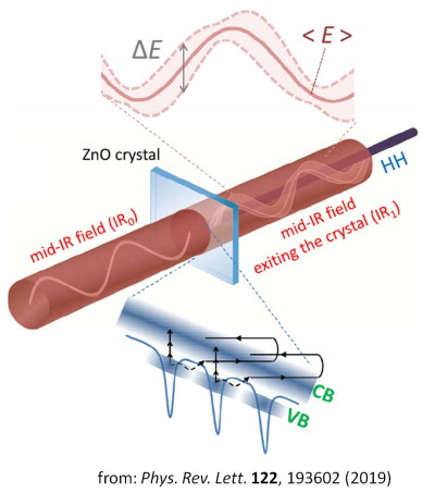
Recently we have developed a theoretical approach for the quantum optical description of strong-field laser-atom interaction [1], which has been followed up by the experimental development of a "Quantum optical XUV spectrometer" [2] used for studies of "sub-cycle quantum electrodynamics of strongly laser-driven semiconductors" [3].
[1] I. A. Gonoskov, et al., Sci. Rep. 6, 32821 (2016).
[2] N. Tsatrafyllis, et al., Nature Commun. 8, 15170 (2017).
[3] N. Tsatrafyllis et al., Phys. Rev. Lett. 122, 193602 (2019).
Principal Investigator
Position Description
ΚΩΔΙΚΟΣ ΘΕΣΗΣ 3α
Πειραματική μελέτη αλληλεπίδρασης ακτινοβολίας λέιζερ με λεπτά υμένια
ΚΩΔΙΚΟΣ ΘΕΣΗΣ 4α
Μη γραμμική απεικόνιση δισδιάστατων υλικών με χρήση Λέιζερ
Για το πλήρες κείμενο της πρόσκλησης ακολουθήστε τον σύνδεσμο 'Related Documents'
Required Qualifications
ΚΩΔΙΚΟΣ ΘΕΣΗΣ 3α
- Διδακτορικό δίπλωμα στην Φυσική
- Εμπειρία στην πειραματική μελέτη αλληλεπίδρασης ύλης-ακτινοβολίας
- Δημοσιεύσεις σχετικές με το αντικείμενο της θέσης
- Άριστη γνώση της Αγγλικής γλώσσας
ΚΩΔΙΚΟΣ ΘΕΣΗΣ 4α
- Πτυχίο Φυσικής
- Μεταπτυχιακός Τίτλος (MSc) σε σχετικό πεδίο με το αντικείμενο της θέσης
- Εμπειρία στην απεικόνιση υλικών με χρήση Λέιζερ
- Άριστη γνώση της Αγγλικής γλώσσας
Application Procedure
Στο φάκελο υποβολής της πρότασης κάθε ενδιαφερόμενου θα πρέπει να εμπεριέχονται τα ακόλουθα:
- Αίτηση (form Greek στην αριστερή στήλη) με αναφορά όνομα του προγράμματος και στον κωδικό της θέσης
- Αναλυτικό Βιογραφικό Σημείωμα
- Ευκρινή φωτοαντίγραφα τίτλων σπουδών
- Πρόσφατη βεβαίωση σπουδών υποψήφιου διδάκτορα για τη θέση 4α
ΥΠΟΒΟΛΗ ΠΡΟΤΑΣΕΩΝ
Οι ενδιαφερόμενοι καλούνται να υποβάλουν τις αιτήσεις τους και όλα τα απαραίτητα δικαιολογητικά, ηλεκτρονικά στη διεύθυνση hr@iesl.forth.gr με κοινοποίηση (cc): στον Δρ Εμμ. Στρατάκη (stratak@iesl.forth.gr).
Οι αιτήσεις θα πρέπει να αποσταλούν με την ένδειξη: «Αίτηση στο πλαίσιο του προγράμματος GRAPH-EYE και της πρόσκλησης εκδήλωσης ενδιαφέροντος με Α.Π. … και κωδικό θέσης … » (όπως αυτός αναφέρεται στον Πίνακα του Παραρτήματος).
Appointment Duration
6 μήνεςPosition Description
Υποστήριξη έρευνας που διεξάγεται στο πλαίσιο του έργου CALLOS «Ανοιχτό Εργαστήριο Συντήρησης των Μνημείων της Αθήνας με τεχνολογίες Λέιζερ και LIDAR» και εστιάζεται στην ανάπτυξη ανοικτού εργαστηρίου συντήρησης αρχαιοτήτων και διαγνωστικών μεθόδων βασιζόμενων σε τεχνολογίες λέιζερ. Ειδικότερα ο/η υποψήφιος/α αναμένεται να έχει ενεργό συμμετοχή σε τεχνολογική έρευνα που στοχεύει στην ανάπτυξη υβριδικών φορητών διαγνωστικών συστημάτων ανάλυσης υλικών σε αρχαιολογικά αντικείμενα και μνημεία με τεχνικές λέιζερ.
Για το πλήρες κείμενο της πρόσκλησης ακολουθήστε τον σύνδεσμο 'Related Documents'
Required Qualifications
- Διδακτορικό στις φυσικές επιστήμες ή την μηχανική (Φυσική, Χημεία, Επιστήμη Υλικών ή συναφή πεδία)
- Υψηλού επιπέδου γνώση και εμπειρία στην εφαρμογή πειραματικών μεθόδων μελέτης φυσικοχημικών διεργασιών και ανάλυσης υλικών με τεχνικές λέιζερ
- Αποδεδειγμένη εμπειρία στην ανάπτυξη και χρήση πειραματικών διατάξεων φασματοσκοπίας λέιζερ (π.χ. LIF, LIBS, κ.α.) στη μελέτη φυσικοχημικών διεργασιών και την ανάλυση υλικών
Desirable Qualifications
- Ερευνητικό/ επιστημονικό έργο μετά την απόκτηση του διδακτορικού (επιστημονικές δημοσιεύσεις και παρουσιάσεις σε συνέδρια με αντικείμενο σχετικό με το έργο)
- Εμπειρία σε διαγνωστικές μεθόδους και τεχνικές με εφαρμογή σε μνημεία και αντικείμενα Πολιτισμικής Κληρονομιάς
- Εμπειρία στη χρήση φασματοσκοπικών μεθόδων για την εξ’ αποστάσεως (remote) μελέτη και ανάλυση υλικών
- Δημοσιεύσεις σε έγκριτα επιστημονικά περιοδικά
Application Procedure
Στο φάκελο υποβολής της πρότασης θα πρέπει να εμπεριέχονται τα ακόλουθα:
- Αίτηση (form Greek στην αριστερή στήλη) με αναφορά στον κωδικό της θέσης
- Αναλυτικό Βιογραφικό Σημείωμα
- Ευκρινή φωτοαντίγραφα τίτλων σπουδών
ΥΠΟΒΟΛΗ ΠΡΟΤΑΣΕΩΝ
Οι ενδιαφερόμενοι καλούνται να υποβάλουν τις αιτήσεις τους και όλα τα απαραίτητα δικαιολογητικά, ηλεκτρονικά στη διεύθυνση hr@iesl.forth.gr με κοινοποίηση (cc): στην Δρ Π. Πουλή (ppouli@iesl.forth.gr).
Οι αιτήσεις θα πρέπει να αποσταλούν με την ένδειξη: «Αίτηση στο πλαίσιο του προγράμματος CALLOS, της πρόσκλησης εκδήλωσης ενδιαφέροντος με Α.Π. … και κωδικό θέσης … » (όπως αυτός αναφέρεται στον Πίνακα του Παραρτήματος).
Appointment Duration
12 μήνεςTo: 01/07/2020 14:00
Τhe discovery and development of conducting polymers not only endowed Heeger, MacDiarmid and Shirakawa with the Nobel Prize in Chemistry 2000 but, more importantly, marked the emergence of Organic Electronics. Polymers are now incorporated in electronic devices that benefit from their (semi)conducting and/or electroactive functionalities, combined with the advantages brought by their soft nature, i.e. flexibility, ease of processing, lightness, etc. Thanks to these merits polymers are now employed in cutting-edge technologies, in applications related to energy harvesting, sensing and actuation, bioelectronics, lighting and others. In this talk I will highlight the links between polymers processing, resulting nanostructure and final functions. I will focus on two families of polymers which are of great interest for organic electronic devices: a) PEDOT-based (semi)conducting materials and, b) PVDF-based ferro-/piezo-electric polymers.
Position Description
Πολαριτονικές δομές GaN και χρήση τους ως πηγές εναγκαλισμένων φωτονίων.
Ο υποψήφιος θα σχεδιάσει, κατασκευάσει και χαρακτηρίσει πολαριτονικές δομές νιτριδίου του γαλλίου με σκοπό την ανίχνευση εναγκαλισμένων φωτονίων που παράγονται από παραμετρικές σκεδάσεις των πολαριτονίων. Οι κύριες τεχνικές που θα χρησιμοποιηθούν είναι αυτές της φωτο-ηλεκτροχημικής χάραξης, της μικρο-φωταύγειας και μικρο-ανακλαστικότητας, και της γωνιακά εξαρτημένης φωταύγειας.
Για το πλήρες κείμενο της πρόσκλησης ακολουθήστε τον σύνδεσμο 'Related Documents'
Required Qualifications
- Πτυχίο Φυσικού, Επιστήμης Υλικών, ή Ηλεκτρολόγου Μηχανικού
- Εμπειρία σε οπτικό, ηλεκτρικό και δομικό χαρακτηρισμό ημιαγωγών νιτριδίου του γαλλίου
- Εμπειρία σε φωτο-ηλεκτροχημική χάραξη μεμβρανών νιτριδίου του γαλλίου
Application Procedure
Στο φάκελο υποβολής της πρότασης θα πρέπει να εμπεριέχονται τα ακόλουθα:
- Αίτηση (form Greek στην αριστερή στήλη) με αναφορά στον κωδικό της θέσης και στο όνομα του προγράμματος
- Αναλυτικό Βιογραφικό Σημείωμα
- Ευκρινή φωτοαντίγραφα τίτλων σπουδών
ΥΠΟΒΟΛΗ ΠΡΟΤΑΣΕΩΝ
Οι ενδιαφερόμενοι καλούνται να υποβάλουν τις αιτήσεις τους και όλα τα απαραίτητα δικαιολογητικά, ηλεκτρονικά στη διεύθυνση hr@iesl.forth.gr με κοινοποίηση (cc): στον καθηγ. Ν. Πελεκάνο (pelekano@materials.uoc.gr).
Οι αιτήσεις θα πρέπει να αποσταλούν με την ένδειξη: «Αίτηση στο πλαίσιο του προγράμματος INNOVATION-EL, της πρόσκλησης εκδήλωσης ενδιαφέροντος με Α.Π. … και κωδικό θέσης … » (όπως αυτός αναφέρεται στον Πίνακα του Παραρτήματος).
Appointment Duration
12 μήνεςPosition Description
Ο μεταπτυχιακός φοιτητής θα απασχοληθεί στα πλαίσια της Ενότητας Εργασίας 2 (ΕΕ2) με την μελέτη υλικών για ανάπτυξη επιστρώματων που θα εμφανίζουν αντισταγονικές ιδιότητες, τον χαρακτηρισμό των υλικών και των επιστρωμάτων και με την μελέτη της υδροφιλικότητας επιστρωμένων πολυμερικών φύλλων.
Για το πλήρες κείμενο της πρόσκλησης ακολουθήστε τον σύνδεσμο 'Related Documents'
Related Project
INGRECO -Required Qualifications
- Πτυχίο φυσικών επιστημών (φυσική, χημεία, επιστήμης υλικών) ή μηχανικού
- Γνώση του αντικειμένου της Επιστήμης Πολυμερών και προηγούμενη εμπειρία σε εργαστήρια μελέτης και χαρακτηρισμού πολυμερών και υβριδικών συστημάτων
- Εμπειρία με την μελέτη επιφανειακών ιδιοτήτων και εξοικείωση με την χρήση σχετικών τεχνικών
- Άριστη γνώση της αγγλικής γλώσσας
Application Procedure
Στο φάκελο υποβολής της πρότασης θα πρέπει να εμπεριέχονται τα ακόλουθα:
- Αίτηση (form Greek στην αριστερή στήλη) με αναφορά στον κωδικό της θέσης και στο όνομα του προγράμματος
- Αναλυτικό Βιογραφικό Σημείωμα
- Ευκρινή φωτοαντίγραφα τίτλων σπουδών
- Πρόσφατη βεβαίωση σπουδών μεταπτυχιακού φοιτητή
ΥΠΟΒΟΛΗ ΠΡΟΤΑΣΕΩΝ
Οι ενδιαφερόμενοι καλούνται να υποβάλουν τις αιτήσεις τους και όλα τα απαραίτητα δικαιολογητικά, ηλεκτρονικά στη διεύθυνση hr@iesl.forth.gr με κοινοποίηση (cc): στην Δρ Κ. Χρυσοπούλου (kiki@iesl.forth.gr).
Οι αιτήσεις θα πρέπει να αποσταλούν με την ένδειξη: «Αίτηση στο πλαίσιο του προγράμματος INGRECO, της πρόσκλησης εκδήλωσης ενδιαφέροντος με Α.Π. … και κωδικό θέσης … » (όπως αυτός αναφέρεται στον Πίνακα του Παραρτήματος).
Appointment Duration
6 μήνεςFunding